Fanrong Lin, Jiawei Liu, Huan Lu, Xin Liu, Ying Liu, Zhili Hu,
Pin Lyu, Zhuhua Zhang, Jens Martin, Wanlin Guo*, Yanpeng Liu*
Adv. Funct. Mater. First published: 02 April 2024
Abstract
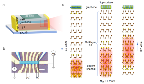
The interface and dielectric environment of graphene transistors are of great importance to commercial circuit integrations. The tangling bond in oxide-based dielectric severely lagged the carrier mobility while the 2D dielectric layer (for instance, hexagonal boron nitride) unavoidably hastened complicated condensed physics even at room temperature. Herein, multilayer black phosphorus (BP) a versatile and widely-tunable dielectric candidate for manifesting graphene fermions is demonstrated. Because of hetero-interfacial charge redistributions, a vertical electric double-layer between the bottom BP layer and top graphene spontaneously forms with the central BP layer as a soft barrier. Under dual-gate modulation, abnormal step-like evolution of Dirac fermions and charge-transfer quantum Hall effect arises while the intrinsic Dirac behavior of graphene is preserved, ascribing to the gate-tunable charge redistributions of dielectric BP layer. Moreover, the electric double-layer transistors apply equally well to bilayer graphene with similar Dirac behavior but an enhanced interfacial charge interference. The findings not only create a new avenue to manipulate the fermions by assembling graphene with narrow-gapped 2D layered materials but also promote electric double-layer transistors as a new build block to design multifunctional devices.

Link:https://onlinelibrary.wiley.com/doi/full/10.1002/adfm.202400553