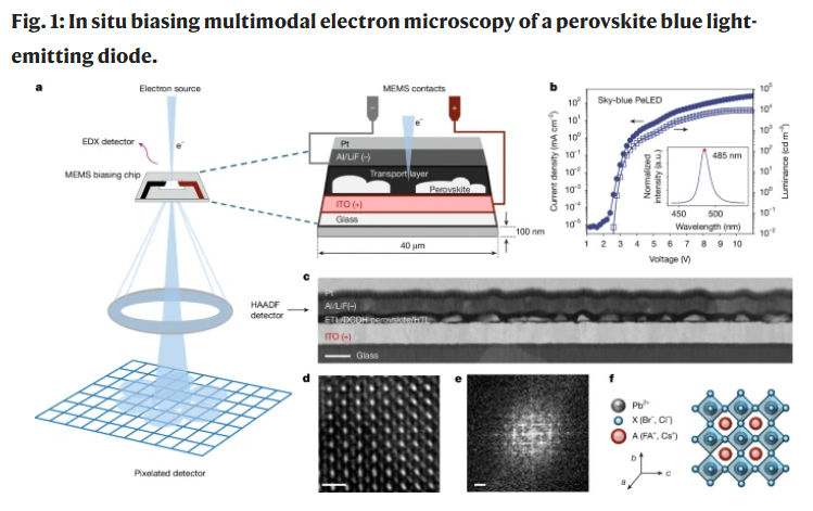
Halide perovskite light-emitting diodes promise high-efficiency1,2,3, low-cost optoelectronics, yet their operational instability remains a critical barrier to practical deployment. Here we develop a multimodal in situ electron microscopy approach that integrates four-dimensional scanning transmission electron microscopy, energy-dispersive X-ray spectroscopy and atomic-resolution imaging to directly visualize structural and chemical evolution in a working halide perovskite light-emitting diode with nanometre precision. Our in situ biasing measurements uncover nanoscale structural and chemical transformations initiated at transport layer interfaces, including the formation of metallic lead and lead-rich secondary phases, as well as strain-driven grain fragmentation. On biasing, we observe the partial transformation of the metallic Al contact to insulating AlCl3. Crucially, whereas the bulk of the perovskite emitter remains relatively intact, our experiment shows that degradation is localized at interfaces. By comparing in situ and ex situ measurements, these results establish a mechanistic link between interfacial strain, ionic transport and electrochemical reactions in working devices, and provide a broadly applicable framework for nanoscale degradation analysis in complex multilayered optoelectronic systems using multimodal in situ biasing microscopy.
https://doi.org/10.1038/s41586-026-10238-8
